标签: ECE425

电子工程代写|超大规模集成电路系统代写Introduction to VLSI Systems代考|CSE435

如果你也在 怎样代写超大规模集成电路系统Introduction to VLSI Systems这个学科遇到相关的难题,请随时右上角联系我们的24/7代写客服。

超大规模集成(VLSI)是通过将成千上万的晶体管合并到一个芯片中来创造集成电路(IC)的过程。VLSI开始于20世纪70年代,当时正在开发复杂的半导体和通信技术。微处理器就是一个VLSI设备。

statistics-lab™ 为您的留学生涯保驾护航 在代写超大规模集成电路系统Introduction to VLSI Systems方面已经树立了自己的口碑, 保证靠谱, 高质且原创的统计Statistics代写服务。我们的专家在代写超大规模集成电路系统Introduction to VLSI Systems方面经验极为丰富,各种代写超大规模集成电路系统Introduction to VLSI Systems相关的作业也就用不着说。

我们提供的超大规模集成电路系统Introduction to VLSI Systems及其相关学科的代写,服务范围广, 其中包括但不限于:

  • Statistical Inference 统计推断
  • Statistical Computing 统计计算
  • Advanced Probability Theory 高等楖率论
  • Advanced Mathematical Statistics 高等数理统计学
  • (Generalized) Linear Models 广义线性模型
  • Statistical Machine Learning 统计机器学习
  • Longitudinal Data Analysis 纵向数据分析
  • Foundations of Data Science 数据科学基础
电子工程代写|超大规模集成电路系统代写Introduction to VLSI Systems代考|CSE435

电子工程代写|超大规模集成电路系统代写Introduction to VLSI Systems代考|CMOS Transmission Gates

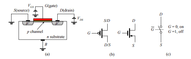
Since a voltage of magnitude $V_{T n}$ between the gate and source of an nMOS transistor is required to turn on the transistor, the maximum output voltage of an $n M O S$ switch is equal to $V_{D D}-V_{T n}$, provided that $V_{D D}$ is applied to both gate and drain electrodes. Similarly, the minimum output voltage of a pMOS switch is equal to $\left|V_{T p}\right|$, provided that $0 \mathrm{~V}$ is applied to both gate and drain electrodes. The above two statements can be restated in terms of information transfer by letting $0 \mathrm{~V}$ represent logic 0 and $V_{D D}$ denote logic 1 as follows. The nMOS transistor can pass 0 perfectly but cannot pass 1 without degradation; the pMOS transistor can pass 1 perfectly but cannot pass 0 without degradation.

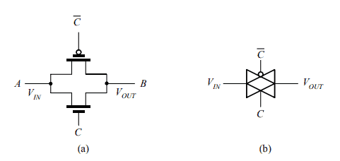
The aforementioned shortcomings of nMOS and pMOS transistors may be overcome by combining an nMOS transistor with a pMOS transistor as a parallel-connected switch, referred to as a transmission gate (TG) or a CMOS switch, as shown in Figure 1.9. Since both nMOS and pMOS transistors are connected in parallel, the imperfect feature of one transistor will be made up by the other. Figure $1.9(\mathrm{a})$ shows the circuit structure of a TG switch and Figure 1.9(b) shows the logic symbol often used in logic diagrams.

Even though using TG switches may overcome the degradation of information passing through them, each TG switch needs two transistors, one nMOS and one pMOS. This means that the use of TG switches needs more area than the use of nMOS switches or pMOS switches alone. In practice, for area-limited applications the use of nMOS transistors is much more prefcrable to pMOS transistors since the clectron mobility is much greater than hole mohility. Hence, nMOS transistors perform much hetter than pMOS transistors.

电子工程代写|超大规模集成电路系统代写Introduction to VLSI Systems代考|Simple Switch Logic Design

As introduced, any of three switches, nMOS, pMOS, and TG, may be used as a switch to control the close (on) or open (off) status of two points. Based on a proper combination of these switches, a switch logic circuit can be constructed. In the following, we begin with the discussion of compound switches and then introduce a systematic design methodology for constructing a switch logic circuit from a given switching function.
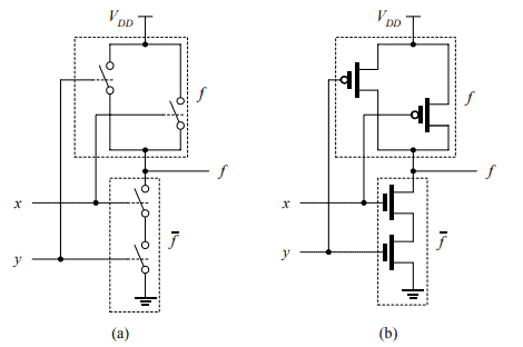
For many applications, we often combine two or more switches in a serial, parallel, or combined fashion to form a compound switch. For instance, the case of two switches being connected in series to form a compound switch is shown in Figure 1.10. The operation of the resulting switch is controlled by two control signals: $S 1$ and $S 2$. The compound switch is turned on only when both control signals $S 1$ and $S 2$ are asserted and remains in an off state otherwise.

Recall that to activate an nMOS switch we need to apply a high-level voltage to its gate and to activate a pMOS switch we need to apply a low-level voltage to its gate. As a result, the compound nMOS switch shown in Figure 1.10(a) is turned on only when both control signals $S 1$ and $S 2$ are at high-level voltages (usually $V_{D D}$ ) and remains in an off state in all other combinations of control signals. The compound pMOS switch depicted in Figure $1.10$ (b) is turned on only when both control signals $S 1$ and $S 2$ are at low-level voltages (usually at the ground level) and remains in an off state in all other combinations of control signals.

Figure $1.11$ shows the case of two switches being connected in parallel to form a compound switch. The operation of the resulting switch is controlled by two control signals: $S 1$ and $S 2$. The compound switch is turned on whenever either switch is on. Therefore, the compound switch is turned off only if both control signals $S 1$ and $S 2$ are deasserted and remains in an on state otherwise.

In Figure 1.11(a), the compound nMOS switch is turned on whenever one control signal of $S 1$ and $S 2$ is at a high-level voltage (usually $V_{D D}$ ) and remains in an off state only when both control signals are at the ground level. In Figure 1.11(b), the compound pMOS switch is turned on whenever one control signal of $S 1$ and $S 2$ is at the ground level and remains in an off state only when both control signals $S 1$ and $S 2$ are at high-level voltages.

电子工程代写|超大规模集成电路系统代写Introduction to VLSI Systems代考|CSE435

超大规模集成电路系统代考

电子工程代写|超大规模集成电路系统代写Introduction to VLSI Systems代考|CMOS Transmission Gates

由于电压幅度在吨n一个nMOS晶体管的栅极和源极之间需要打开晶体管,一个的最大输出电压n米○小号开关等于在DD−在吨n, 前提是在DD应用于栅极和漏极。类似地,pMOS 开关的最小输出电压等于|在吨p|, 前提是0 在应用于栅极和漏极。上述两个陈述在信息传递方面可以通过让0 在表示逻辑 0 和在DD如下表示逻辑1。nMOS晶体管可以完美通过0但不能通过1而不退化;pMOS晶体管可以完美地通过1,但不能通过0而不退化。

上述 nMOS 和 pMOS 晶体管的缺点可以通过将 nMOS 晶体管与 pMOS 晶体管组合为并联开关(称为传输门 (TG) 或 CMOS 开关)来克服,如图 1.9 所示。由于nMOS和pMOS晶体管都是并联的,一个晶体管的不完善特性将由另一个晶体管来弥补。数字1.9(一个)图 1.9(b) 显示了 TG 开关的电路结构,图 1.9(b) 显示了逻辑图中常用的逻辑符号。

尽管使用 TG 开关可以克服通过它们的信息的劣化,但每个 TG 开关需要两个晶体管,一个 nMOS 和一个 pMOS。这意味着使用 TG 开关比单独使用 nMOS 开关或 pMOS 开关需要更多的面积。实际上,对于面积受限的应用,使用 nMOS 晶体管比使用 pMOS 晶体管更可取,因为电子迁移率远大于空穴迁移率。因此,nMOS 晶体管的性能比 pMOS 晶体管好得多。

电子工程代写|超大规模集成电路系统代写Introduction to VLSI Systems代考|Simple Switch Logic Design

如前所述,nMOS、pMOS和TG这三个开关中的任何一个都可以用作开关来控制两点的闭合(开)或开(关)状态。基于这些开关的适当组合,可以构建开关逻辑电路。下面,我们首先讨论复合开关,然后介绍一种系统设计方法,用于根据给定的开关功能构建开关逻辑电路。
对于许多应用,我们经常将两个或多个开关以串行、并行或组合的方式组合起来,形成一个复合开关。例如,两个开关串联形成复合开关的情况如图 1.10 所示。生成的开关的操作由两个控制信号控制:小号1和小号2. 只有当两个控制信号都打开复合开关小号1和小号2被断言并保持在关闭状态,否则。

回想一下,要激活 nMOS 开关,我们需要向其栅极施加高电平电压,而要激活 pMOS 开关,我们需要向其栅极施加低电平电压。结果,图 1.10(a) 所示的复合 nMOS 开关仅在两个控制信号小号1和小号2处于高电平电压(通常在DD) 并在所有其他控制信号组合中保持关闭状态。如图所示的复合 pMOS 开关1.10(b) 仅当两个控制信号都打开小号1和小号2处于低电平电压(通常处于地电平)并且在所有其他控制信号组合中保持关闭状态。

数字1.11显示了两个开关并联形成复合开关的情况。生成的开关的操作由两个控制信号控制:小号1和小号2. 只要任一开关打开,复合开关就会打开。因此,只有当两个控制信号都关闭复合开关小号1和小号2被置低,否则保持开启状态。

在图 1.11(a) 中,只要一个控制信号为小号1和小号2处于高电平电压(通常在DD) 并且仅当两个控制信号都处于地电平时才保持关闭状态。在图 1.11(b) 中,只要一个控制信号小号1和小号2处于地电平并且仅当两个控制信号都保持在关闭状态小号1和小号2处于高电平电压。

电子工程代写|超大规模集成电路系统代写Introduction to VLSI Systems代考 请认准statistics-lab™

统计代写请认准statistics-lab™. statistics-lab™为您的留学生涯保驾护航。统计代写|python代写代考

随机过程代考

在概率论概念中,随机过程随机变量的集合。 若一随机系统的样本点是随机函数,则称此函数为样本函数,这一随机系统全部样本函数的集合是一个随机过程。 实际应用中,样本函数的一般定义在时间域或者空间域。 随机过程的实例如股票和汇率的波动、语音信号、视频信号、体温的变化,随机运动如布朗运动、随机徘徊等等。

贝叶斯方法代考

贝叶斯统计概念及数据分析表示使用概率陈述回答有关未知参数的研究问题以及统计范式。后验分布包括关于参数的先验分布,和基于观测数据提供关于参数的信息似然模型。根据选择的先验分布和似然模型,后验分布可以解析或近似,例如,马尔科夫链蒙特卡罗 (MCMC) 方法之一。贝叶斯统计概念及数据分析使用后验分布来形成模型参数的各种摘要,包括点估计,如后验平均值、中位数、百分位数和称为可信区间的区间估计。此外,所有关于模型参数的统计检验都可以表示为基于估计后验分布的概率报表。

广义线性模型代考

广义线性模型(GLM)归属统计学领域,是一种应用灵活的线性回归模型。该模型允许因变量的偏差分布有除了正态分布之外的其它分布。

statistics-lab作为专业的留学生服务机构,多年来已为美国、英国、加拿大、澳洲等留学热门地的学生提供专业的学术服务,包括但不限于Essay代写,Assignment代写,Dissertation代写,Report代写,小组作业代写,Proposal代写,Paper代写,Presentation代写,计算机作业代写,论文修改和润色,网课代做,exam代考等等。写作范围涵盖高中,本科,研究生等海外留学全阶段,辐射金融,经济学,会计学,审计学,管理学等全球99%专业科目。写作团队既有专业英语母语作者,也有海外名校硕博留学生,每位写作老师都拥有过硬的语言能力,专业的学科背景和学术写作经验。我们承诺100%原创,100%专业,100%准时,100%满意。

机器学习代写

随着AI的大潮到来,Machine Learning逐渐成为一个新的学习热点。同时与传统CS相比,Machine Learning在其他领域也有着广泛的应用,因此这门学科成为不仅折磨CS专业同学的“小恶魔”,也是折磨生物、化学、统计等其他学科留学生的“大魔王”。学习Machine learning的一大绊脚石在于使用语言众多,跨学科范围广,所以学习起来尤其困难。但是不管你在学习Machine Learning时遇到任何难题,StudyGate专业导师团队都能为你轻松解决。

多元统计分析代考


基础数据: $N$ 个样本, $P$ 个变量数的单样本,组成的横列的数据表
变量定性: 分类和顺序;变量定量:数值
数学公式的角度分为: 因变量与自变量

时间序列分析代写

随机过程,是依赖于参数的一组随机变量的全体,参数通常是时间。 随机变量是随机现象的数量表现,其时间序列是一组按照时间发生先后顺序进行排列的数据点序列。通常一组时间序列的时间间隔为一恒定值(如1秒,5分钟,12小时,7天,1年),因此时间序列可以作为离散时间数据进行分析处理。研究时间序列数据的意义在于现实中,往往需要研究某个事物其随时间发展变化的规律。这就需要通过研究该事物过去发展的历史记录,以得到其自身发展的规律。

回归分析代写

多元回归分析渐进(Multiple Regression Analysis Asymptotics)属于计量经济学领域,主要是一种数学上的统计分析方法,可以分析复杂情况下各影响因素的数学关系,在自然科学、社会和经济学等多个领域内应用广泛。

MATLAB代写

MATLAB 是一种用于技术计算的高性能语言。它将计算、可视化和编程集成在一个易于使用的环境中,其中问题和解决方案以熟悉的数学符号表示。典型用途包括:数学和计算算法开发建模、仿真和原型制作数据分析、探索和可视化科学和工程图形应用程序开发,包括图形用户界面构建MATLAB 是一个交互式系统,其基本数据元素是一个不需要维度的数组。这使您可以解决许多技术计算问题,尤其是那些具有矩阵和向量公式的问题,而只需用 C 或 Fortran 等标量非交互式语言编写程序所需的时间的一小部分。MATLAB 名称代表矩阵实验室。MATLAB 最初的编写目的是提供对由 LINPACK 和 EISPACK 项目开发的矩阵软件的轻松访问,这两个项目共同代表了矩阵计算软件的最新技术。MATLAB 经过多年的发展,得到了许多用户的投入。在大学环境中,它是数学、工程和科学入门和高级课程的标准教学工具。在工业领域,MATLAB 是高效研究、开发和分析的首选工具。MATLAB 具有一系列称为工具箱的特定于应用程序的解决方案。对于大多数 MATLAB 用户来说非常重要,工具箱允许您学习应用专业技术。工具箱是 MATLAB 函数(M 文件)的综合集合,可扩展 MATLAB 环境以解决特定类别的问题。可用工具箱的领域包括信号处理、控制系统、神经网络、模糊逻辑、小波、仿真等。

R语言代写问卷设计与分析代写
PYTHON代写回归分析与线性模型代写
MATLAB代写方差分析与试验设计代写
STATA代写机器学习/统计学习代写
SPSS代写计量经济学代写
EVIEWS代写时间序列分析代写
EXCEL代写深度学习代写
SQL代写各种数据建模与可视化代写

电子工程代写|超大规模集成电路系统代写Introduction to VLSI Systems代考|ECE5745

如果你也在 怎样代写超大规模集成电路系统Introduction to VLSI Systems这个学科遇到相关的难题,请随时右上角联系我们的24/7代写客服。

超大规模集成(VLSI)是通过将成千上万的晶体管合并到一个芯片中来创造集成电路(IC)的过程。VLSI开始于20世纪70年代,当时正在开发复杂的半导体和通信技术。微处理器就是一个VLSI设备。

statistics-lab™ 为您的留学生涯保驾护航 在代写超大规模集成电路系统Introduction to VLSI Systems方面已经树立了自己的口碑, 保证靠谱, 高质且原创的统计Statistics代写服务。我们的专家在代写超大规模集成电路系统Introduction to VLSI Systems方面经验极为丰富,各种代写超大规模集成电路系统Introduction to VLSI Systems相关的作业也就用不着说。

我们提供的超大规模集成电路系统Introduction to VLSI Systems及其相关学科的代写,服务范围广, 其中包括但不限于:

  • Statistical Inference 统计推断
  • Statistical Computing 统计计算
  • Advanced Probability Theory 高等楖率论
  • Advanced Mathematical Statistics 高等数理统计学
  • (Generalized) Linear Models 广义线性模型
  • Statistical Machine Learning 统计机器学习
  • Longitudinal Data Analysis 纵向数据分析
  • Foundations of Data Science 数据科学基础
电子工程代写|超大规模集成电路系统代写Introduction to VLSI Systems代考|ECE5745

电子工程代写|超大规模集成电路系统代写Introduction to VLSI Systems代考|nMOS Transistors

The physical structure of an nMOS transistor is basically composed of a metal-oxidesilicon (MOS) system and two $n^{+}$regions on the surface of a p-type silicon substrate, as depicted in Figure 1.7(a). The MOS system is a sandwich structure where a dielectric (an insulator) is inserted between a metal or a polysilicon and a p-type substrate. The metal or polysilicon is called the gate. The two $n^{+}$regions on the surface of the substrate are referred to as drain and source, respectively.

The operation of an nMOS transistor can hee illustrated by Figure $1.7(\mathrm{a})$. When a large enough positive voltage $V_{G S}$ is applied to the gate (electrode), electrons are attracted toward the silicon surface from the $p$-type substrate due to a positive electric field being built on the silicon surface by the gate voltage. These electrons form a channel between the drain and source. The minimum voltage $V_{G S}$ inducing the channel is defined as the threshold voltage, denoted $V_{T n}$, of the nMOS transistor. The value of $V_{T n}$ ranges from $0.3 \mathrm{~V}$ to $0.7 \mathrm{~V}$ for the present submicron and deep-submicron processes, depending on a particular process of interest.

For digital applications, an nMOS transistor can be thought of as a simple switch element. The switch is turned on when the gate voltage is greater than or equal to its threshold voltage and turned off otherwise. Due to the symmetric structure of an nMOS transistor, either of $n^{+}$regions can be used as the source or drain, depending on how the operating voltage is applied. One with more positive voltage is the drain and the other is the source because the carriers on the nMOS transistor are electrons.
Figure $1.7$ (b) shows the circuit symbols that are often used in circuit designs. The one with an explicit arrow associated with the source electrode is often used in analog applications, where the roles of source and drain are fixed. The other without an explicit arrow is often used in digital applications because the roles of the drain and source will be dynamically determined by the actual operating conditions of the circuit. The switch circuit model is depicted in Figure $1.7(\mathrm{c})$.

电子工程代写|超大规模集成电路系统代写Introduction to VLSI Systems代考|pMOS Transistors

Likewise, the physical structure of a pMOS transistor comprises a MOS system and two $p^{+}$regions on the surface of an $n$-type silicon substrate, as depicted in Figure $1.8(\mathrm{a})$. The MOS system is a sandwich structure where a dielectric (an insulator) is inserted between a metal or polysilicon and an $n$-type substrate. The metal or polysilicon is called a gate. The two $p^{+}$regions on the surface of substrate are referred to as the drain and source, respectively.

The operation of a pMOS transistor can be illustrated by Figure 1.8(a). When a large negative voltage $V_{G S}$ is applied to the gate (electrode), holes are attracted toward the silicon surface from the $n$-type substrate due to a negative electric field being built on the silicon surface by the gate voltage. These holes form a channel between the drain and source. The minimum voltage $\left|V_{G S}\right|$ inducing the channel is defined as the threshold vollage, denoted $V_{T p}$, of the pMOS Lransistor. The value of $V_{T p}$ ranges from $-0.3 \mathrm{~V}$ to $-0.7 \mathrm{~V}$ for the present submicron and deep-submicron processes, depending on a particular process of interest.

Like an nMOS transistor, a pMOS transistor can be regarded as a simple switch element for digital applications. The switch is turned on when the gate voltage is less than or equal to its threshold voltage and turned off otherwise. Due to the symmetric structure of a pMOS transistor, either of $p^{+}$regions can be used as the source or drain, depending on how the operating voltage is applied. One with more positive voltage is the source and the other is the drain since the carriers on the pMOS transistor are holes.

Figure 1.8(b) shows the circuit symbols that are often used in circuit designs. The symbol convention of pMOS transistors is exactly the same as that of nMOS transistors. The one with an explicit arrow associated with the source electrode is often used in analog applications in which the roles of source and drain are fixed. The other without an explicit arrow but with a circle at the gate is often used in digital applications because the roles of drain and source will be dynamically determined by the actual operating conditions of the circuit. The circle is used to distinguish it from the nMOS transistor and to indicate that the pMOS transistor is at active-low cnable. The switch circuit model is depicted in Figure $1.8(\mathrm{c})$.

电子工程代写|超大规模集成电路系统代写Introduction to VLSI Systems代考|ECE5745

超大规模集成电路系统代考

电子工程代写|超大规模集成电路系统代写Introduction to VLSI Systems代考|nMOS Transistors

nMOS晶体管的物理结构基本上由一个金属氧化物硅(MOS)系统和两个n+p 型硅衬底表面上的区域,如图 1.7(a) 所示。MOS系统是一种夹层结构,其中在金属或多晶硅和p型衬底之间插入了电介质(绝缘体)。金属或多晶硅称为栅极。他们俩n+衬底表面上的区域分别称为漏极和源极。

nMOS晶体管的操作可以用图来说明1.7(一个). 当足够大的正电压在G小号施加到栅极(电极),电子从硅表面被吸引p型衬底由于栅极电压在硅表面上建立了正电场。这些电子在漏极和源极之间形成通道。最低电压在G小号诱导通道被定义为阈值电压,表示在吨n, nMOS 晶体管。的价值在吨n范围从0.3 在至0.7 在对于目前的亚微米和深亚微米工艺,取决于感兴趣的特定工艺。

对于数字应用,nMOS 晶体管可以被认为是一个简单的开关元件。当栅极电压大于或等于其阈值电压时,开关打开,否则关闭。由于 nMOS 晶体管的对称结构,n+区域可用作源极或漏极,具体取决于施加工作电压的方式。一个具有更大正电压的是漏极,另一个是源极,因为 nMOS 晶体管上的载流子是电子。
数字1.7(b) 显示了电路设计中经常使用的电路符号。与源电极相关的带有明确箭头的箭头通常用于模拟应用中,其中源极和漏极的角色是固定的。另一个没有明确箭头的通常用于数字应用中,因为漏极和源极的角色将由电路的实际工作条件动态确定。开关电路模型如图所示1.7(C).

电子工程代写|超大规模集成电路系统代写Introduction to VLSI Systems代考|pMOS Transistors

同样,pMOS 晶体管的物理结构包括一个 MOS 系统和两个p+表面上的区域n型硅衬底,如图所示1.8(一个). MOS系统是一种夹层结构,其中在金属或多晶硅和金属之间插入了电介质(绝缘体)。n型基板。金属或多晶硅称为栅极。他们俩p+衬底表面上的区域分别称为漏极和源极。

图 1.8(a) 可以说明 pMOS 晶体管的操作。当一个大的负电压在G小号被施加到栅极(电极),空穴被吸引到硅表面从n型衬底由于栅极电压在硅表面上建立了负电场。这些孔在漏极和源极之间形成通道。最低电压|在G小号|诱导通道被定义为阈值电压,表示为在吨p,的 pMOS 晶体管。的价值在吨p范围从−0.3 在至−0.7 在对于目前的亚微米和深亚微米工艺,取决于感兴趣的特定工艺。

与 nMOS 晶体管一样,pMOS 晶体管可被视为数字应用的简单开关元件。当栅极电压小于或等于其阈值电压时,开关打开,否则关闭。由于 pMOS 晶体管的对称结构,p+区域可用作源极或漏极,具体取决于施加工作电压的方式。由于 pMOS 晶体管上的载流子是空穴,因此具有更大正电压的一个是源极,另一个是漏极。

图 1.8(b) 显示了电路设计中经常使用的电路符号。pMOS晶体管的符号约定与nMOS晶体管的符号约定完全相同。与源电极相关的带有明确箭头的箭头通常用于源极和漏极的角色固定的模拟应用中。另一个没有明确箭头但在栅极有一个圆圈的方法通常用于数字应用中,因为漏极和源极的角色将由电路的实际工作条件动态确定。圆圈用来与nMOS晶体管区分开来,表示pMOS晶体管处于低电平有效。开关电路模型如图所示1.8(C).

电子工程代写|超大规模集成电路系统代写Introduction to VLSI Systems代考 请认准statistics-lab™

统计代写请认准statistics-lab™. statistics-lab™为您的留学生涯保驾护航。统计代写|python代写代考

随机过程代考

在概率论概念中,随机过程随机变量的集合。 若一随机系统的样本点是随机函数,则称此函数为样本函数,这一随机系统全部样本函数的集合是一个随机过程。 实际应用中,样本函数的一般定义在时间域或者空间域。 随机过程的实例如股票和汇率的波动、语音信号、视频信号、体温的变化,随机运动如布朗运动、随机徘徊等等。

贝叶斯方法代考

贝叶斯统计概念及数据分析表示使用概率陈述回答有关未知参数的研究问题以及统计范式。后验分布包括关于参数的先验分布,和基于观测数据提供关于参数的信息似然模型。根据选择的先验分布和似然模型,后验分布可以解析或近似,例如,马尔科夫链蒙特卡罗 (MCMC) 方法之一。贝叶斯统计概念及数据分析使用后验分布来形成模型参数的各种摘要,包括点估计,如后验平均值、中位数、百分位数和称为可信区间的区间估计。此外,所有关于模型参数的统计检验都可以表示为基于估计后验分布的概率报表。

广义线性模型代考

广义线性模型(GLM)归属统计学领域,是一种应用灵活的线性回归模型。该模型允许因变量的偏差分布有除了正态分布之外的其它分布。

statistics-lab作为专业的留学生服务机构,多年来已为美国、英国、加拿大、澳洲等留学热门地的学生提供专业的学术服务,包括但不限于Essay代写,Assignment代写,Dissertation代写,Report代写,小组作业代写,Proposal代写,Paper代写,Presentation代写,计算机作业代写,论文修改和润色,网课代做,exam代考等等。写作范围涵盖高中,本科,研究生等海外留学全阶段,辐射金融,经济学,会计学,审计学,管理学等全球99%专业科目。写作团队既有专业英语母语作者,也有海外名校硕博留学生,每位写作老师都拥有过硬的语言能力,专业的学科背景和学术写作经验。我们承诺100%原创,100%专业,100%准时,100%满意。

机器学习代写

随着AI的大潮到来,Machine Learning逐渐成为一个新的学习热点。同时与传统CS相比,Machine Learning在其他领域也有着广泛的应用,因此这门学科成为不仅折磨CS专业同学的“小恶魔”,也是折磨生物、化学、统计等其他学科留学生的“大魔王”。学习Machine learning的一大绊脚石在于使用语言众多,跨学科范围广,所以学习起来尤其困难。但是不管你在学习Machine Learning时遇到任何难题,StudyGate专业导师团队都能为你轻松解决。

多元统计分析代考


基础数据: $N$ 个样本, $P$ 个变量数的单样本,组成的横列的数据表
变量定性: 分类和顺序;变量定量:数值
数学公式的角度分为: 因变量与自变量

时间序列分析代写

随机过程,是依赖于参数的一组随机变量的全体,参数通常是时间。 随机变量是随机现象的数量表现,其时间序列是一组按照时间发生先后顺序进行排列的数据点序列。通常一组时间序列的时间间隔为一恒定值(如1秒,5分钟,12小时,7天,1年),因此时间序列可以作为离散时间数据进行分析处理。研究时间序列数据的意义在于现实中,往往需要研究某个事物其随时间发展变化的规律。这就需要通过研究该事物过去发展的历史记录,以得到其自身发展的规律。

回归分析代写

多元回归分析渐进(Multiple Regression Analysis Asymptotics)属于计量经济学领域,主要是一种数学上的统计分析方法,可以分析复杂情况下各影响因素的数学关系,在自然科学、社会和经济学等多个领域内应用广泛。

MATLAB代写

MATLAB 是一种用于技术计算的高性能语言。它将计算、可视化和编程集成在一个易于使用的环境中,其中问题和解决方案以熟悉的数学符号表示。典型用途包括:数学和计算算法开发建模、仿真和原型制作数据分析、探索和可视化科学和工程图形应用程序开发,包括图形用户界面构建MATLAB 是一个交互式系统,其基本数据元素是一个不需要维度的数组。这使您可以解决许多技术计算问题,尤其是那些具有矩阵和向量公式的问题,而只需用 C 或 Fortran 等标量非交互式语言编写程序所需的时间的一小部分。MATLAB 名称代表矩阵实验室。MATLAB 最初的编写目的是提供对由 LINPACK 和 EISPACK 项目开发的矩阵软件的轻松访问,这两个项目共同代表了矩阵计算软件的最新技术。MATLAB 经过多年的发展,得到了许多用户的投入。在大学环境中,它是数学、工程和科学入门和高级课程的标准教学工具。在工业领域,MATLAB 是高效研究、开发和分析的首选工具。MATLAB 具有一系列称为工具箱的特定于应用程序的解决方案。对于大多数 MATLAB 用户来说非常重要,工具箱允许您学习应用专业技术。工具箱是 MATLAB 函数(M 文件)的综合集合,可扩展 MATLAB 环境以解决特定类别的问题。可用工具箱的领域包括信号处理、控制系统、神经网络、模糊逻辑、小波、仿真等。

R语言代写问卷设计与分析代写
PYTHON代写回归分析与线性模型代写
MATLAB代写方差分析与试验设计代写
STATA代写机器学习/统计学习代写
SPSS代写计量经济学代写
EVIEWS代写时间序列分析代写
EXCEL代写深度学习代写
SQL代写各种数据建模与可视化代写

电子工程代写|超大规模集成电路系统代写Introduction to VLSI Systems代考|ECE1192

如果你也在 怎样代写超大规模集成电路系统Introduction to VLSI Systems这个学科遇到相关的难题,请随时右上角联系我们的24/7代写客服。

超大规模集成(VLSI)是通过将成千上万的晶体管合并到一个芯片中来创造集成电路(IC)的过程。VLSI开始于20世纪70年代,当时正在开发复杂的半导体和通信技术。微处理器就是一个VLSI设备。

statistics-lab™ 为您的留学生涯保驾护航 在代写超大规模集成电路系统Introduction to VLSI Systems方面已经树立了自己的口碑, 保证靠谱, 高质且原创的统计Statistics代写服务。我们的专家在代写超大规模集成电路系统Introduction to VLSI Systems方面经验极为丰富,各种代写超大规模集成电路系统Introduction to VLSI Systems相关的作业也就用不着说。

我们提供的超大规模集成电路系统Introduction to VLSI Systems及其相关学科的代写,服务范围广, 其中包括但不限于:

  • Statistical Inference 统计推断
  • Statistical Computing 统计计算
  • Advanced Probability Theory 高等楖率论
  • Advanced Mathematical Statistics 高等数理统计学
  • (Generalized) Linear Models 广义线性模型
  • Statistical Machine Learning 统计机器学习
  • Longitudinal Data Analysis 纵向数据分析
  • Foundations of Data Science 数据科学基础
电子工程代写|超大规模集成电路系统代写Introduction to VLSI Systems代考|ECE1192

电子工程代写|超大规模集成电路系统代写Introduction to VLSI Systems代考|Design Issues of VLSI Circuits

A VLSI manufacturing process is called a submicron $(\mathrm{SM})$ process when the feature size is below $1 \mu \mathrm{m}$, and a deep submicron (DSM) process when the feature size is roughly below $0.25 \mu \mathrm{m}^{2}$ The corresponding devices made by these two processes are denoted SM devices and DSM devices, respectively. At present, DSM devices are popular in the design of a large-scale system because they provide a more economical way to integrate a much more complicated system into a single chip. The resulting chip is often referred to as a system-on-a-chip (SoC) device.

Even though DSM processes allow us to design a very complicated large-scale system, many design challenges indeed exist, in particular, when the feature sizes are beyond $0.13 \mu \mathrm{m}$. The associated design issues can be subdivided into two main classes: DSM devices and DSM interconnect. ${ }^{3}$ In the following, we address each of these briefly.

The design issues of DSM devices include thin-oxide (gate-oxide) tunneling/breakdown, gate leakage current, subthreshold current, velocity saturation, short-channel effects on $V_{T}$, hot-carrier effects, and draininduced barrier lowering (DIBL) effect.

The device features of typical DSM processes are summarized in Table $1.1$. From the table, we can see that the thin-oxide (gate-oxide, i.e., silicon dioxide, $\mathrm{SiO}_{2}$ ) thickness is reduced from $5.7 \mathrm{~nm}$ in a $0.25-\mu \mathrm{m}$ process down to $1.65 \mathrm{~nm}$ in a $32-\mathrm{nm}$ process. The side effects of this reduction are thin-oxide tunneling and breakdown. The thin-oxide tunneling may cause an extra gate leakage current. To avoid thin-oxide breakdown, the operating voltage applied to the gate has to be lowered. This means that the noise margins are reduced accordingly and the subthreshold current may no longer be ignored. To reduce the gate leakage current, high- $k$ MOS transistors are widely employed starting from a $45-\mathrm{nm}$ process. In high- $k$ MOS transistors, a high- $k$ dielectric is used to replace the gate oxide. Hence, the gate-dielectric thickness may be increased significantly, thereby reducing the gate leakage current dramatically. The actual gatedielectric thickness depends on the relative permittivity of gate-dielectric material, referring to Section 3.4.1.2 for more details.

In addition, as the channel length of a device is reduced, velocity saturation, shortchannel effects on $V_{T}$, and hot-carrier effects may no longer be ignored as in the case of a long-channel device. The electron and hole velocities in the channel or silicon bulk is proportional to the applied electric field when the electric field is below a critical value. However, these velocities will saturate at a value of about $8 \times 10^{6} \mathrm{~cm} / \mathrm{sec}$ at 400 $\mathrm{K}$, which is independent of the doping level and corresponds to an electric field with the strength of $6 \times 10^{4} \mathrm{~V} / \mathrm{cm}$ for electrons and $2.4 \times 10^{5} \mathrm{~V} / \mathrm{cm}$ for holes, respectively. When velocity saturation happens, the drain current of a MOS transistor will follow a linear rather than a quadratical relationship with applied gate-to-source voltage.

电子工程代写|超大规模集成电路系统代写Introduction to VLSI Systems代考|Economics of VLSI

The cost of an IC is roughly composed of two major factors: fixed cost and variable cost. The fixed cost, also referred to as the nonrecurring engineering (NRE) cost, is independent of the sales volume. It is mainly contributed by the cost from that a project is started until the first successful prototype is obtained. More precisely, the fixed cost covers direct and indirect costs. The direct cost includes the research and design (R\&D) cost, manufacturing mask cost, as well as marketing and sales cost; the indirect cost comprises the investment of manufacturing equipments, the investment of CAD tools, building infrastructure cost, and so on. The variable cost is proportional to the product volume and is mainly the cost of manufacturing wafers, namely, wafer price, which is roughly in the range between 1,200 and 1,600 USD for a 300 -mm wafer.

From the above discussion, the cost per IC can be expressed as follows.
Cost per $\mathrm{IC}=$ Variable cost of $\mathrm{IC}+\frac{\text { Fixed cost }}{\text { Volume }}$
The variable cost per IC can be formulated as the following equation.
Variable cost of $\mathrm{IC}=$
Cost of die $+$ Cost of testing die $+$ Cost of packaging and final test
Final test yield $\times$ Dies per wafer
The cost of a die is the wafer price divided by the number of good dies and can be represented as the following formula.
$$
\text { Cost of die }=\frac{\text { Wafer price }}{\text { Dies per wafer } \times \text { Die yield }}
$$
The number of dies in a wafer, excluding fragmented dies on the boundary, can be approximated by the following equation.
Dies per wafer $=\frac{3}{4} \frac{d^{2}}{A}-\frac{1}{2 \sqrt{A}} d$
where $d$ is the diameter of the wafer and $A$ is the area of square dies. The derivation of this equation is left to the reader as an exercise.
The die yield can be estimated by the following widely used function.
Die yield $=\left(1+\frac{D_{0} A}{\alpha}\right)^{-\alpha}$
where $D_{0}$ is the defect density, i.e., the defects per unit area, in defects $/ \mathrm{cm}^{2}$, and $\alpha$ is a measure of manufacturing complexity. The typical values of $D_{0}$ and $\alpha$ are $0.3$ to $1.3$ and $4.0$, respectively. From this equation, it is clear that the die yield is inversely proportional to the die area.

The following two examples exemplify the above concepts about the cost of an IC. In these two examples, we intend to ignore the fixed cost and only take into account the wafer price when calculating die cost.

电子工程代写|超大规模集成电路系统代写Introduction to VLSI Systems代考|ECE1192

超大规模集成电路系统代考

电子工程代写|超大规模集成电路系统代写Introduction to VLSI Systems代考|Design Issues of VLSI Circuits

超大规模集成电路制造过程称为亚微米(小号米)当特征尺寸低于1米米,当特征尺寸大致低于0.25米米2这两个过程所对应的设备分别记为SM设备和DSM设备。目前,DSM 器件在大规模系统设计中很流行,因为它们提供了一种更经济的方式将更复杂的系统集成到单个芯片中。由此产生的芯片通常被称为片上系统 (SoC) 设备。

尽管 DSM 流程允许我们设计一个非常复杂的大型系统,但确实存在许多设计挑战,特别是当特征尺寸超出0.13米米. 相关的设计问题可以细分为两大类:DSM 设备和 DSM 互连。3在下文中,我们将简要介绍其中的每一个。

DSM 器件的设计问题包括薄氧化物 (gate-oxide) 隧穿/击穿、栅极漏电流、亚阈值电流、速度饱和、在吨,热载流子效应和漏极降低势垒(DIBL)效应。

典型 DSM 工艺的器件特性总结于表中1.1. 从表中可以看出,薄氧化物(栅极氧化物,即二氧化硅,小号一世○2) 厚度从5.7 n米在一个0.25−米米处理到1.65 n米在一个32−n米过程。这种减少的副作用是薄氧化物隧道效应和击穿。薄氧化物隧穿可能导致额外的栅极漏电流。为了避免薄氧化物击穿,必须降低施加到栅极的工作电压。这意味着噪声容限会相应降低,并且可能不再忽略亚阈值电流。为了减少栅极漏电流,高ķMOS晶体管被广泛采用从一个开始45−n米过程。在高ķMOS晶体管,一个高ķ电介质用于代替栅极氧化物。因此,可以显着增加栅极电介质厚度,从而显着降低栅极漏电流。实际的栅介质厚度取决于栅介质材料的相对介电常数,有关详细信息,请参阅第 3.4.1.2 节。

此外,随着器件通道长度的缩短,速度饱和、短通道对器件的影响在吨,并且热载流子效应可能不再像长通道器件那样被忽略。当电场低于临界值时,沟道或硅块中的电子和空穴速度与施加的电场成比例。然而,这些速度将在大约8×10⁶ C米/s和C在 400ķ,它与掺杂水平无关,对应于强度为6×10⁴ 在/C米对于电子和2.4×105 在/C米分别为孔。当速度饱和发生时,MOS 晶体管的漏极电流将与施加的栅源电压呈线性关系,而不是二次关系。

电子工程代写|超大规模集成电路系统代写Introduction to VLSI Systems代考|Economics of VLSI

$I C$ 的成本大致由两个主要因素组成:固定成本和可变成本。固定成本,也称为非经常性工程 (NRE) 成本,与销量无 关。它主要来自从项目启动到获得第一个成功原型的成本。更准确地说,固定成本包括直接成本和间接成本。直接 成本包括研究和设计 (RI\&D) 成本、制造掩模成本,以及营销和销售成本;间接成本包括制造设备投资、CAD工 具投资、基础设施建设成本等。可变成本与产品数量成正比,主要是制造晶圆的成本,即晶圆价格, 300 毫米晶圆 大致在1200-1600美元之间。
根据上述讨论,每个 $I C$ 的成本可以表示如下。
每次成本 $\mathrm{IC}=$ 可变成本 $\mathrm{IC}+\frac{\text { Fixed cost }}{\text { Volume }}$
每个 $I C$ 的可变成本可以表示为以下等式。
可变成本 $\mathrm{IC}=$
模具成本十测试模具的成本十封装成本和最终测试
最终测试良率×每个晶圆
的裸片 裸片的成本是晶圆价格除以优质裸片的数量,可以表示为以下公式。
$$
\text { Cost of die }=\frac{\text { Wafer price }}{\text { Dies per wafer } \times \text { Die yield }}
$$
晶片中的管芯数量 (不包括边界上的碎片管芯) 可以通过以下等式近似。
每个晶圆的裸片 $=\frac{3}{4} \frac{d^{2}}{A}-\frac{1}{2 \sqrt{A}} d$
在哪里 $d$ 是晶片的直径和 $A$ 是方形模具的面积。这个方程的推导留给读者作为练习。
可以通过以下广泛使用的函数来估计裸片良率。
模具产量 $=\left(1+\frac{D_{0} A}{\alpha}\right)^{-\alpha}$
在哪里 $D_{0}$ 是缺陷密度,即单位面积的缺陷数,在缺陷中 $/ \mathrm{cm}^{2}$ ,和 $\alpha$ 是衡量制造复杂性的指标。的典型值 $D_{0}$ 和 $\alpha$ 是 $0.3$ 至 $1.3$ 和 $4.0$ ,分别。从这个等式可以清楚地看出,裸片良率与裸片面积成反比。
以下两个示例举例说明了上述有关 IC 成本的概念。在这两个例子中,我们打算忽略固定成本,在计算裸片成本时 只考虑晶圆价格。

电子工程代写|超大规模集成电路系统代写Introduction to VLSI Systems代考 请认准statistics-lab™

统计代写请认准statistics-lab™. statistics-lab™为您的留学生涯保驾护航。统计代写|python代写代考

随机过程代考

在概率论概念中,随机过程随机变量的集合。 若一随机系统的样本点是随机函数,则称此函数为样本函数,这一随机系统全部样本函数的集合是一个随机过程。 实际应用中,样本函数的一般定义在时间域或者空间域。 随机过程的实例如股票和汇率的波动、语音信号、视频信号、体温的变化,随机运动如布朗运动、随机徘徊等等。

贝叶斯方法代考

贝叶斯统计概念及数据分析表示使用概率陈述回答有关未知参数的研究问题以及统计范式。后验分布包括关于参数的先验分布,和基于观测数据提供关于参数的信息似然模型。根据选择的先验分布和似然模型,后验分布可以解析或近似,例如,马尔科夫链蒙特卡罗 (MCMC) 方法之一。贝叶斯统计概念及数据分析使用后验分布来形成模型参数的各种摘要,包括点估计,如后验平均值、中位数、百分位数和称为可信区间的区间估计。此外,所有关于模型参数的统计检验都可以表示为基于估计后验分布的概率报表。

广义线性模型代考

广义线性模型(GLM)归属统计学领域,是一种应用灵活的线性回归模型。该模型允许因变量的偏差分布有除了正态分布之外的其它分布。

statistics-lab作为专业的留学生服务机构,多年来已为美国、英国、加拿大、澳洲等留学热门地的学生提供专业的学术服务,包括但不限于Essay代写,Assignment代写,Dissertation代写,Report代写,小组作业代写,Proposal代写,Paper代写,Presentation代写,计算机作业代写,论文修改和润色,网课代做,exam代考等等。写作范围涵盖高中,本科,研究生等海外留学全阶段,辐射金融,经济学,会计学,审计学,管理学等全球99%专业科目。写作团队既有专业英语母语作者,也有海外名校硕博留学生,每位写作老师都拥有过硬的语言能力,专业的学科背景和学术写作经验。我们承诺100%原创,100%专业,100%准时,100%满意。

机器学习代写

随着AI的大潮到来,Machine Learning逐渐成为一个新的学习热点。同时与传统CS相比,Machine Learning在其他领域也有着广泛的应用,因此这门学科成为不仅折磨CS专业同学的“小恶魔”,也是折磨生物、化学、统计等其他学科留学生的“大魔王”。学习Machine learning的一大绊脚石在于使用语言众多,跨学科范围广,所以学习起来尤其困难。但是不管你在学习Machine Learning时遇到任何难题,StudyGate专业导师团队都能为你轻松解决。

多元统计分析代考


基础数据: $N$ 个样本, $P$ 个变量数的单样本,组成的横列的数据表
变量定性: 分类和顺序;变量定量:数值
数学公式的角度分为: 因变量与自变量

时间序列分析代写

随机过程,是依赖于参数的一组随机变量的全体,参数通常是时间。 随机变量是随机现象的数量表现,其时间序列是一组按照时间发生先后顺序进行排列的数据点序列。通常一组时间序列的时间间隔为一恒定值(如1秒,5分钟,12小时,7天,1年),因此时间序列可以作为离散时间数据进行分析处理。研究时间序列数据的意义在于现实中,往往需要研究某个事物其随时间发展变化的规律。这就需要通过研究该事物过去发展的历史记录,以得到其自身发展的规律。

回归分析代写

多元回归分析渐进(Multiple Regression Analysis Asymptotics)属于计量经济学领域,主要是一种数学上的统计分析方法,可以分析复杂情况下各影响因素的数学关系,在自然科学、社会和经济学等多个领域内应用广泛。

MATLAB代写

MATLAB 是一种用于技术计算的高性能语言。它将计算、可视化和编程集成在一个易于使用的环境中,其中问题和解决方案以熟悉的数学符号表示。典型用途包括:数学和计算算法开发建模、仿真和原型制作数据分析、探索和可视化科学和工程图形应用程序开发,包括图形用户界面构建MATLAB 是一个交互式系统,其基本数据元素是一个不需要维度的数组。这使您可以解决许多技术计算问题,尤其是那些具有矩阵和向量公式的问题,而只需用 C 或 Fortran 等标量非交互式语言编写程序所需的时间的一小部分。MATLAB 名称代表矩阵实验室。MATLAB 最初的编写目的是提供对由 LINPACK 和 EISPACK 项目开发的矩阵软件的轻松访问,这两个项目共同代表了矩阵计算软件的最新技术。MATLAB 经过多年的发展,得到了许多用户的投入。在大学环境中,它是数学、工程和科学入门和高级课程的标准教学工具。在工业领域,MATLAB 是高效研究、开发和分析的首选工具。MATLAB 具有一系列称为工具箱的特定于应用程序的解决方案。对于大多数 MATLAB 用户来说非常重要,工具箱允许您学习应用专业技术。工具箱是 MATLAB 函数(M 文件)的综合集合,可扩展 MATLAB 环境以解决特定类别的问题。可用工具箱的领域包括信号处理、控制系统、神经网络、模糊逻辑、小波、仿真等。

R语言代写问卷设计与分析代写
PYTHON代写回归分析与线性模型代写
MATLAB代写方差分析与试验设计代写
STATA代写机器学习/统计学习代写
SPSS代写计量经济学代写
EVIEWS代写时间序列分析代写
EXCEL代写深度学习代写
SQL代写各种数据建模与可视化代写