电气工程代写|数字电路代写digital circuit代考|ECEN6003
如果你也在 怎样代写数字电路digital circuit这个学科遇到相关的难题,请随时右上角联系我们的24/7代写客服。
数字电子学是电子学的一个领域,涉及数字信号的研究和使用或产生数字信号的设备工程。这与模拟电子学和模拟信号相反。
statistics-lab™ 为您的留学生涯保驾护航 在代写数字电路digital circuit方面已经树立了自己的口碑, 保证靠谱, 高质且原创的统计Statistics代写服务。我们的专家在代写数字电路digital circuit代写方面经验极为丰富,各种代写数字电路digital circuit相关的作业也就用不着说。
我们提供的数字电路digital circuit及其相关学科的代写,服务范围广, 其中包括但不限于:
- Statistical Inference 统计推断
- Statistical Computing 统计计算
- Advanced Probability Theory 高等概率论
- Advanced Mathematical Statistics 高等数理统计学
- (Generalized) Linear Models 广义线性模型
- Statistical Machine Learning 统计机器学习
- Longitudinal Data Analysis 纵向数据分析
- Foundations of Data Science 数据科学基础
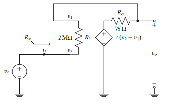
电气工程代写|数字电路代写digital circuit代考|INVERTING AMPLIFIER
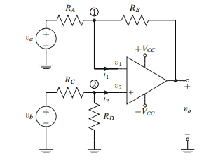
The inverting amplifier configuration shown in Figure $1.11$ amplifies and inverts the input signal in the linear region of operation. The circuit consists of a resistor $R_S$ in series with the voltage source $v_i$ connected to the inverting input of the OpAmp. The non-inverting input of the OpAmp is short circuited to ground (common). A resistor $R_f$ is connected to the output and provides a negative feedback path to the inverting input terminal. ${ }^{12}$ Because the output resistance of the OpAmp is nearly zero, the output voltage $v_o$ will not depend on the current that might be supplied to a load resistor connected between the output and ground.
For most OpAmps, it is appropriate to assume that their characteristics are approximated closely by the ideal OpAmp model of Section 1.2. Therefore, analysis of the inverting amplifier can proceed using the voltage and current constraints of Equations ( $1.5 \mathrm{a})$ and ( $1.5 \mathrm{~b})$,
Node 1 is said to be a virtual ground due to the virtual short circuit between the inverting and non-inverting terminals (which is grounded) as defined by the voltage constraint,
$$
v_1=v_2=0 .
$$
The node voltage method of analysis is applied at node 1 ,
$$
0=\frac{v_i-v_1}{R_S}+\frac{v_0-v_1}{R_f}+i_1 .
$$
By applying Equation (1.25), obtained from the virtual short circuit, and the constraint on the current $i_1$ as defined in Equation (1.5b), Equation (1.26) is simplified to
$$
0=\frac{v_i}{R_S}+\frac{v_o}{R_f} .
$$
Solving for the voltage gain, $v_o / v_i$,
$$
\frac{v_o}{v_i}=-\frac{R_f}{R_S}
$$
Notice that the voltage gain is dependent only on the ratio of the resistors external to the OpAmp, $R_f$ and $R_S$. The amplifier increases the amplitude of the input signal by this ratio. The negative sign in the voltage gain indicates an inversion in the signal.
The output voltage is also constrained by the supply voltages $V_{C C}$ and $-V_{C C}$,
$$
\left|v_o\right|<V_{C C} \text {. }
$$
Using Equation (1.28), the maximum resistor ratio $R_f / R_s$ for a given input voltage $v_i$ is
$$
\frac{R_f}{R_S}<\left|\frac{V_{C C}}{v_i}\right| .
$$
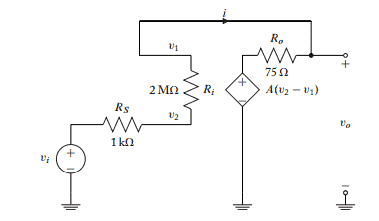
电气工程代写|数字电路代写digital circuit代考|NON-INVERTING AMPLIFIER
A non-inverting amplifier is shown in Figure $1.15$ where the source is represented by $v_S$ and a series resistance $R_S$.
The analysis of the non-inverting amplifier in Figure $1.15$ assumes an ideal OpAmp operating within its linear region. The voltage and current constraints at the input to the OpAmp yield the voltage at node 1 ,
$$
v_1=v_2=v_s,
$$
since $i_1=i_2=0$. Using the node voltage method of analysis, the sum of the currents flowing into node 1 is,
$$
0=\frac{0-v_1}{R_G}+\frac{v_o-v_1}{R_f} .
$$
Solving for the output voltage $v_o$ using the voltage constraints, $v_1=v_S$
$$
v_o=v_i\left(1+\frac{R_f}{R_G}\right) .
$$
The gain of the non-inverting amplifier is,
$$
\frac{v_o}{v_i}=1+\frac{R_f}{R_G} .
$$
Unlike the inverting amplifier, the non-inverting amplifier gain is positive. Therefore, the output and input signals are ideally in phase. The amplifier will operate in its linear region when,
$$
1+\frac{R_f}{R_G}<\left|\frac{V_{C C}}{n_s}\right| .
$$
Note that, like the inverting amplifier, the gain is a function of the external resistors $R_f$ and $R_G$.
数字电路代考
电气工程代写|数字电路代写digital circuit代考|INVERTING AMPLIFIER
反相放大器配置如图 $1.11$ 放大和反转线性工作区域中的输入信号。该电路由一个电阻器组成 $R_S$ 与电压源串联 $v_i$ 连 接到运算放大器的反相输入。OpAmp 的同相输入对地短路 (公共端) 。一个电阻 $R_f$ 连接到输出并为反相输入端 提供负反馈路径。 ${ }^{12}$ 由于运算放大器的输出电阻几乎为零,输出电压 $v_o$ 将不取决于可能提供给连接在输出和地之间 的负载电阻器的电流。
对于大多数运算放大器,假设它们的特性与第 $1.2$ 节的理想运算放大器模型非常接近是合适的。因此,可以使用方 程式 (1.5a)和 $(1.5 \mathrm{~b})$ ,
由于电压约束定义的反相和非反相端子 (接地) 之间的虚拟短路,节点 1 被称为虚拟接地,
$$
v_1=v_2=0 .
$$
节点电压分析方法应用于节点 1 ,
$$
0=\frac{v_i-v_1}{R_S}+\frac{v_0-v_1}{R_f}+i_1 .
$$
通过应用方程 (1.25),从虚拟短路得到,对电流的约束 $i_1$ 如公式 (1.5b) 中定义的,公式 (1.26) 简化为
$$
0=\frac{v_i}{R_S}+\frac{v_o}{R_f} .
$$
求解电压增益, $v_o / v_i$ ,
$$
\frac{v_o}{v_i}=-\frac{R_f}{R_S}
$$
请注意,电压增益仅取决于运算放大器外部电阻器的比率, $R_f$ 和 $R_S$. 放大器通过这个比率增加输入信号的幅度。 电压增益中的负号表示信号反转。
输出电压也受电源电压的限制 $V_{C C}$ 和 $-V_{C C}$ ,
$$
\left|v_o\right|<V_{C C} .
$$
使用公式 (1.28),最大电阻比 $R_f / R_s$ 对于给定的输入电压 $v_i$ 是 $\frac{R_f}{R_S}<\left|\frac{V_{C C}}{v_i}\right|$.
电气工程代写|数字电路代写digital circuit代考|NON-INVERTING AMPLIFIER
同相放大器如图所示 $1.15$ 源表示为 $v_S$ 和一个串联电阻 $R_S$.
图中同相放大器的分析1.15假设一个理想的运算放大器在其线性区域内运行。运算放大器输入端的电压和电流约 束产生节点 1 的电压,
$$
v_1=v_2=v_s,
$$
自从 $i_1=i_2=0$. 使用节点电压分析法,流入节点 1 的电流之和为,
$$
0=\frac{0-v_1}{R_G}+\frac{v_o-v_1}{R_f} .
$$
求解输出电压 $v_o$ 使用电压约束, $v_1=v_S$
$$
v_o=v_i\left(1+\frac{R_f}{R_G}\right)
$$
同相放大器的增益为,
$$
\frac{v_o}{v_i}=1+\frac{R_f}{R_G} .
$$
与反相放大器不同,同相放大器增益为正。因此,输出和输入信号理想地是同相的。放大器将在其线性区域工作, 当,
$$
1+\frac{R_f}{R_G}<\left|\frac{V_{C C}}{n_s}\right| .
$$
请注意,与反相放大器一样,增益是外部电阻器的函数 $R_f$ 和 $R_G$.

统计代写请认准statistics-lab™. statistics-lab™为您的留学生涯保驾护航。
金融工程代写
金融工程是使用数学技术来解决金融问题。金融工程使用计算机科学、统计学、经济学和应用数学领域的工具和知识来解决当前的金融问题,以及设计新的和创新的金融产品。
非参数统计代写
非参数统计指的是一种统计方法,其中不假设数据来自于由少数参数决定的规定模型;这种模型的例子包括正态分布模型和线性回归模型。
广义线性模型代考
广义线性模型(GLM)归属统计学领域,是一种应用灵活的线性回归模型。该模型允许因变量的偏差分布有除了正态分布之外的其它分布。
术语 广义线性模型(GLM)通常是指给定连续和/或分类预测因素的连续响应变量的常规线性回归模型。它包括多元线性回归,以及方差分析和方差分析(仅含固定效应)。
有限元方法代写
有限元方法(FEM)是一种流行的方法,用于数值解决工程和数学建模中出现的微分方程。典型的问题领域包括结构分析、传热、流体流动、质量运输和电磁势等传统领域。
有限元是一种通用的数值方法,用于解决两个或三个空间变量的偏微分方程(即一些边界值问题)。为了解决一个问题,有限元将一个大系统细分为更小、更简单的部分,称为有限元。这是通过在空间维度上的特定空间离散化来实现的,它是通过构建对象的网格来实现的:用于求解的数值域,它有有限数量的点。边界值问题的有限元方法表述最终导致一个代数方程组。该方法在域上对未知函数进行逼近。[1] 然后将模拟这些有限元的简单方程组合成一个更大的方程系统,以模拟整个问题。然后,有限元通过变化微积分使相关的误差函数最小化来逼近一个解决方案。
tatistics-lab作为专业的留学生服务机构,多年来已为美国、英国、加拿大、澳洲等留学热门地的学生提供专业的学术服务,包括但不限于Essay代写,Assignment代写,Dissertation代写,Report代写,小组作业代写,Proposal代写,Paper代写,Presentation代写,计算机作业代写,论文修改和润色,网课代做,exam代考等等。写作范围涵盖高中,本科,研究生等海外留学全阶段,辐射金融,经济学,会计学,审计学,管理学等全球99%专业科目。写作团队既有专业英语母语作者,也有海外名校硕博留学生,每位写作老师都拥有过硬的语言能力,专业的学科背景和学术写作经验。我们承诺100%原创,100%专业,100%准时,100%满意。
随机分析代写
随机微积分是数学的一个分支,对随机过程进行操作。它允许为随机过程的积分定义一个关于随机过程的一致的积分理论。这个领域是由日本数学家伊藤清在第二次世界大战期间创建并开始的。
时间序列分析代写
随机过程,是依赖于参数的一组随机变量的全体,参数通常是时间。 随机变量是随机现象的数量表现,其时间序列是一组按照时间发生先后顺序进行排列的数据点序列。通常一组时间序列的时间间隔为一恒定值(如1秒,5分钟,12小时,7天,1年),因此时间序列可以作为离散时间数据进行分析处理。研究时间序列数据的意义在于现实中,往往需要研究某个事物其随时间发展变化的规律。这就需要通过研究该事物过去发展的历史记录,以得到其自身发展的规律。
回归分析代写
多元回归分析渐进(Multiple Regression Analysis Asymptotics)属于计量经济学领域,主要是一种数学上的统计分析方法,可以分析复杂情况下各影响因素的数学关系,在自然科学、社会和经济学等多个领域内应用广泛。
MATLAB代写
MATLAB 是一种用于技术计算的高性能语言。它将计算、可视化和编程集成在一个易于使用的环境中,其中问题和解决方案以熟悉的数学符号表示。典型用途包括:数学和计算算法开发建模、仿真和原型制作数据分析、探索和可视化科学和工程图形应用程序开发,包括图形用户界面构建MATLAB 是一个交互式系统,其基本数据元素是一个不需要维度的数组。这使您可以解决许多技术计算问题,尤其是那些具有矩阵和向量公式的问题,而只需用 C 或 Fortran 等标量非交互式语言编写程序所需的时间的一小部分。MATLAB 名称代表矩阵实验室。MATLAB 最初的编写目的是提供对由 LINPACK 和 EISPACK 项目开发的矩阵软件的轻松访问,这两个项目共同代表了矩阵计算软件的最新技术。MATLAB 经过多年的发展,得到了许多用户的投入。在大学环境中,它是数学、工程和科学入门和高级课程的标准教学工具。在工业领域,MATLAB 是高效研究、开发和分析的首选工具。MATLAB 具有一系列称为工具箱的特定于应用程序的解决方案。对于大多数 MATLAB 用户来说非常重要,工具箱允许您学习和应用专业技术。工具箱是 MATLAB 函数(M 文件)的综合集合,可扩展 MATLAB 环境以解决特定类别的问题。可用工具箱的领域包括信号处理、控制系统、神经网络、模糊逻辑、小波、仿真等。