如果你也在 怎样代写超大规模集成电路系统Introduction to VLSI Systems这个学科遇到相关的难题,请随时右上角联系我们的24/7代写客服。
超大规模集成(VLSI)是通过将成千上万的晶体管合并到一个芯片中来创造集成电路(IC)的过程。VLSI开始于20世纪70年代,当时正在开发复杂的半导体和通信技术。微处理器就是一个VLSI设备。
statistics-lab™ 为您的留学生涯保驾护航 在代写超大规模集成电路系统Introduction to VLSI Systems方面已经树立了自己的口碑, 保证靠谱, 高质且原创的统计Statistics代写服务。我们的专家在代写超大规模集成电路系统Introduction to VLSI Systems方面经验极为丰富,各种代写超大规模集成电路系统Introduction to VLSI Systems相关的作业也就用不着说。
我们提供的超大规模集成电路系统Introduction to VLSI Systems及其相关学科的代写,服务范围广, 其中包括但不限于:
- Statistical Inference 统计推断
- Statistical Computing 统计计算
- Advanced Probability Theory 高等楖率论
- Advanced Mathematical Statistics 高等数理统计学
- (Generalized) Linear Models 广义线性模型
- Statistical Machine Learning 统计机器学习
- Longitudinal Data Analysis 纵向数据分析
- Foundations of Data Science 数据科学基础
电子工程代写|超大规模集成电路系统代写Introduction to VLSI Systems代考|Design Issues of VLSI Circuits
A VLSI manufacturing process is called a submicron $(\mathrm{SM})$ process when the feature size is below $1 \mu \mathrm{m}$, and a deep submicron (DSM) process when the feature size is roughly below $0.25 \mu \mathrm{m}^{2}$ The corresponding devices made by these two processes are denoted SM devices and DSM devices, respectively. At present, DSM devices are popular in the design of a large-scale system because they provide a more economical way to integrate a much more complicated system into a single chip. The resulting chip is often referred to as a system-on-a-chip (SoC) device.
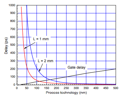
Even though DSM processes allow us to design a very complicated large-scale system, many design challenges indeed exist, in particular, when the feature sizes are beyond $0.13 \mu \mathrm{m}$. The associated design issues can be subdivided into two main classes: DSM devices and DSM interconnect. ${ }^{3}$ In the following, we address each of these briefly.
The design issues of DSM devices include thin-oxide (gate-oxide) tunneling/breakdown, gate leakage current, subthreshold current, velocity saturation, short-channel effects on $V_{T}$, hot-carrier effects, and draininduced barrier lowering (DIBL) effect.
The device features of typical DSM processes are summarized in Table $1.1$. From the table, we can see that the thin-oxide (gate-oxide, i.e., silicon dioxide, $\mathrm{SiO}_{2}$ ) thickness is reduced from $5.7 \mathrm{~nm}$ in a $0.25-\mu \mathrm{m}$ process down to $1.65 \mathrm{~nm}$ in a $32-\mathrm{nm}$ process. The side effects of this reduction are thin-oxide tunneling and breakdown. The thin-oxide tunneling may cause an extra gate leakage current. To avoid thin-oxide breakdown, the operating voltage applied to the gate has to be lowered. This means that the noise margins are reduced accordingly and the subthreshold current may no longer be ignored. To reduce the gate leakage current, high- $k$ MOS transistors are widely employed starting from a $45-\mathrm{nm}$ process. In high- $k$ MOS transistors, a high- $k$ dielectric is used to replace the gate oxide. Hence, the gate-dielectric thickness may be increased significantly, thereby reducing the gate leakage current dramatically. The actual gatedielectric thickness depends on the relative permittivity of gate-dielectric material, referring to Section 3.4.1.2 for more details.
In addition, as the channel length of a device is reduced, velocity saturation, shortchannel effects on $V_{T}$, and hot-carrier effects may no longer be ignored as in the case of a long-channel device. The electron and hole velocities in the channel or silicon bulk is proportional to the applied electric field when the electric field is below a critical value. However, these velocities will saturate at a value of about $8 \times 10^{6} \mathrm{~cm} / \mathrm{sec}$ at 400 $\mathrm{K}$, which is independent of the doping level and corresponds to an electric field with the strength of $6 \times 10^{4} \mathrm{~V} / \mathrm{cm}$ for electrons and $2.4 \times 10^{5} \mathrm{~V} / \mathrm{cm}$ for holes, respectively. When velocity saturation happens, the drain current of a MOS transistor will follow a linear rather than a quadratical relationship with applied gate-to-source voltage.
电子工程代写|超大规模集成电路系统代写Introduction to VLSI Systems代考|Economics of VLSI
The cost of an IC is roughly composed of two major factors: fixed cost and variable cost. The fixed cost, also referred to as the nonrecurring engineering (NRE) cost, is independent of the sales volume. It is mainly contributed by the cost from that a project is started until the first successful prototype is obtained. More precisely, the fixed cost covers direct and indirect costs. The direct cost includes the research and design (R\&D) cost, manufacturing mask cost, as well as marketing and sales cost; the indirect cost comprises the investment of manufacturing equipments, the investment of CAD tools, building infrastructure cost, and so on. The variable cost is proportional to the product volume and is mainly the cost of manufacturing wafers, namely, wafer price, which is roughly in the range between 1,200 and 1,600 USD for a 300 -mm wafer.
From the above discussion, the cost per IC can be expressed as follows.
Cost per $\mathrm{IC}=$ Variable cost of $\mathrm{IC}+\frac{\text { Fixed cost }}{\text { Volume }}$
The variable cost per IC can be formulated as the following equation.
Variable cost of $\mathrm{IC}=$
Cost of die $+$ Cost of testing die $+$ Cost of packaging and final test
Final test yield $\times$ Dies per wafer
The cost of a die is the wafer price divided by the number of good dies and can be represented as the following formula.
$$
\text { Cost of die }=\frac{\text { Wafer price }}{\text { Dies per wafer } \times \text { Die yield }}
$$
The number of dies in a wafer, excluding fragmented dies on the boundary, can be approximated by the following equation.
Dies per wafer $=\frac{3}{4} \frac{d^{2}}{A}-\frac{1}{2 \sqrt{A}} d$
where $d$ is the diameter of the wafer and $A$ is the area of square dies. The derivation of this equation is left to the reader as an exercise.
The die yield can be estimated by the following widely used function.
Die yield $=\left(1+\frac{D_{0} A}{\alpha}\right)^{-\alpha}$
where $D_{0}$ is the defect density, i.e., the defects per unit area, in defects $/ \mathrm{cm}^{2}$, and $\alpha$ is a measure of manufacturing complexity. The typical values of $D_{0}$ and $\alpha$ are $0.3$ to $1.3$ and $4.0$, respectively. From this equation, it is clear that the die yield is inversely proportional to the die area.
The following two examples exemplify the above concepts about the cost of an IC. In these two examples, we intend to ignore the fixed cost and only take into account the wafer price when calculating die cost.
超大规模集成电路系统代考
电子工程代写|超大规模集成电路系统代写Introduction to VLSI Systems代考|Design Issues of VLSI Circuits
超大规模集成电路制造过程称为亚微米(小号米)当特征尺寸低于1米米,当特征尺寸大致低于0.25米米2这两个过程所对应的设备分别记为SM设备和DSM设备。目前,DSM 器件在大规模系统设计中很流行,因为它们提供了一种更经济的方式将更复杂的系统集成到单个芯片中。由此产生的芯片通常被称为片上系统 (SoC) 设备。
尽管 DSM 流程允许我们设计一个非常复杂的大型系统,但确实存在许多设计挑战,特别是当特征尺寸超出0.13米米. 相关的设计问题可以细分为两大类:DSM 设备和 DSM 互连。3在下文中,我们将简要介绍其中的每一个。
DSM 器件的设计问题包括薄氧化物 (gate-oxide) 隧穿/击穿、栅极漏电流、亚阈值电流、速度饱和、在吨,热载流子效应和漏极降低势垒(DIBL)效应。
典型 DSM 工艺的器件特性总结于表中1.1. 从表中可以看出,薄氧化物(栅极氧化物,即二氧化硅,小号一世○2) 厚度从5.7 n米在一个0.25−米米处理到1.65 n米在一个32−n米过程。这种减少的副作用是薄氧化物隧道效应和击穿。薄氧化物隧穿可能导致额外的栅极漏电流。为了避免薄氧化物击穿,必须降低施加到栅极的工作电压。这意味着噪声容限会相应降低,并且可能不再忽略亚阈值电流。为了减少栅极漏电流,高ķMOS晶体管被广泛采用从一个开始45−n米过程。在高ķMOS晶体管,一个高ķ电介质用于代替栅极氧化物。因此,可以显着增加栅极电介质厚度,从而显着降低栅极漏电流。实际的栅介质厚度取决于栅介质材料的相对介电常数,有关详细信息,请参阅第 3.4.1.2 节。
此外,随着器件通道长度的缩短,速度饱和、短通道对器件的影响在吨,并且热载流子效应可能不再像长通道器件那样被忽略。当电场低于临界值时,沟道或硅块中的电子和空穴速度与施加的电场成比例。然而,这些速度将在大约8×10⁶ C米/s和C在 400ķ,它与掺杂水平无关,对应于强度为6×10⁴ 在/C米对于电子和2.4×105 在/C米分别为孔。当速度饱和发生时,MOS 晶体管的漏极电流将与施加的栅源电压呈线性关系,而不是二次关系。
电子工程代写|超大规模集成电路系统代写Introduction to VLSI Systems代考|Economics of VLSI
$I C$ 的成本大致由两个主要因素组成:固定成本和可变成本。固定成本,也称为非经常性工程 (NRE) 成本,与销量无 关。它主要来自从项目启动到获得第一个成功原型的成本。更准确地说,固定成本包括直接成本和间接成本。直接 成本包括研究和设计 (RI\&D) 成本、制造掩模成本,以及营销和销售成本;间接成本包括制造设备投资、CAD工 具投资、基础设施建设成本等。可变成本与产品数量成正比,主要是制造晶圆的成本,即晶圆价格, 300 毫米晶圆 大致在1200-1600美元之间。
根据上述讨论,每个 $I C$ 的成本可以表示如下。
每次成本 $\mathrm{IC}=$ 可变成本 $\mathrm{IC}+\frac{\text { Fixed cost }}{\text { Volume }}$
每个 $I C$ 的可变成本可以表示为以下等式。
可变成本 $\mathrm{IC}=$
模具成本十测试模具的成本十封装成本和最终测试
最终测试良率×每个晶圆
的裸片 裸片的成本是晶圆价格除以优质裸片的数量,可以表示为以下公式。
$$
\text { Cost of die }=\frac{\text { Wafer price }}{\text { Dies per wafer } \times \text { Die yield }}
$$
晶片中的管芯数量 (不包括边界上的碎片管芯) 可以通过以下等式近似。
每个晶圆的裸片 $=\frac{3}{4} \frac{d^{2}}{A}-\frac{1}{2 \sqrt{A}} d$
在哪里 $d$ 是晶片的直径和 $A$ 是方形模具的面积。这个方程的推导留给读者作为练习。
可以通过以下广泛使用的函数来估计裸片良率。
模具产量 $=\left(1+\frac{D_{0} A}{\alpha}\right)^{-\alpha}$
在哪里 $D_{0}$ 是缺陷密度,即单位面积的缺陷数,在缺陷中 $/ \mathrm{cm}^{2}$ ,和 $\alpha$ 是衡量制造复杂性的指标。的典型值 $D_{0}$ 和 $\alpha$ 是 $0.3$ 至 $1.3$ 和 $4.0$ ,分别。从这个等式可以清楚地看出,裸片良率与裸片面积成反比。
以下两个示例举例说明了上述有关 IC 成本的概念。在这两个例子中,我们打算忽略固定成本,在计算裸片成本时 只考虑晶圆价格。

统计代写请认准statistics-lab™. statistics-lab™为您的留学生涯保驾护航。统计代写|python代写代考
随机过程代考
在概率论概念中,随机过程是随机变量的集合。 若一随机系统的样本点是随机函数,则称此函数为样本函数,这一随机系统全部样本函数的集合是一个随机过程。 实际应用中,样本函数的一般定义在时间域或者空间域。 随机过程的实例如股票和汇率的波动、语音信号、视频信号、体温的变化,随机运动如布朗运动、随机徘徊等等。
贝叶斯方法代考
贝叶斯统计概念及数据分析表示使用概率陈述回答有关未知参数的研究问题以及统计范式。后验分布包括关于参数的先验分布,和基于观测数据提供关于参数的信息似然模型。根据选择的先验分布和似然模型,后验分布可以解析或近似,例如,马尔科夫链蒙特卡罗 (MCMC) 方法之一。贝叶斯统计概念及数据分析使用后验分布来形成模型参数的各种摘要,包括点估计,如后验平均值、中位数、百分位数和称为可信区间的区间估计。此外,所有关于模型参数的统计检验都可以表示为基于估计后验分布的概率报表。
广义线性模型代考
广义线性模型(GLM)归属统计学领域,是一种应用灵活的线性回归模型。该模型允许因变量的偏差分布有除了正态分布之外的其它分布。
statistics-lab作为专业的留学生服务机构,多年来已为美国、英国、加拿大、澳洲等留学热门地的学生提供专业的学术服务,包括但不限于Essay代写,Assignment代写,Dissertation代写,Report代写,小组作业代写,Proposal代写,Paper代写,Presentation代写,计算机作业代写,论文修改和润色,网课代做,exam代考等等。写作范围涵盖高中,本科,研究生等海外留学全阶段,辐射金融,经济学,会计学,审计学,管理学等全球99%专业科目。写作团队既有专业英语母语作者,也有海外名校硕博留学生,每位写作老师都拥有过硬的语言能力,专业的学科背景和学术写作经验。我们承诺100%原创,100%专业,100%准时,100%满意。
机器学习代写
随着AI的大潮到来,Machine Learning逐渐成为一个新的学习热点。同时与传统CS相比,Machine Learning在其他领域也有着广泛的应用,因此这门学科成为不仅折磨CS专业同学的“小恶魔”,也是折磨生物、化学、统计等其他学科留学生的“大魔王”。学习Machine learning的一大绊脚石在于使用语言众多,跨学科范围广,所以学习起来尤其困难。但是不管你在学习Machine Learning时遇到任何难题,StudyGate专业导师团队都能为你轻松解决。
多元统计分析代考
基础数据: $N$ 个样本, $P$ 个变量数的单样本,组成的横列的数据表
变量定性: 分类和顺序;变量定量:数值
数学公式的角度分为: 因变量与自变量
时间序列分析代写
随机过程,是依赖于参数的一组随机变量的全体,参数通常是时间。 随机变量是随机现象的数量表现,其时间序列是一组按照时间发生先后顺序进行排列的数据点序列。通常一组时间序列的时间间隔为一恒定值(如1秒,5分钟,12小时,7天,1年),因此时间序列可以作为离散时间数据进行分析处理。研究时间序列数据的意义在于现实中,往往需要研究某个事物其随时间发展变化的规律。这就需要通过研究该事物过去发展的历史记录,以得到其自身发展的规律。
回归分析代写
多元回归分析渐进(Multiple Regression Analysis Asymptotics)属于计量经济学领域,主要是一种数学上的统计分析方法,可以分析复杂情况下各影响因素的数学关系,在自然科学、社会和经济学等多个领域内应用广泛。
MATLAB代写
MATLAB 是一种用于技术计算的高性能语言。它将计算、可视化和编程集成在一个易于使用的环境中,其中问题和解决方案以熟悉的数学符号表示。典型用途包括:数学和计算算法开发建模、仿真和原型制作数据分析、探索和可视化科学和工程图形应用程序开发,包括图形用户界面构建MATLAB 是一个交互式系统,其基本数据元素是一个不需要维度的数组。这使您可以解决许多技术计算问题,尤其是那些具有矩阵和向量公式的问题,而只需用 C 或 Fortran 等标量非交互式语言编写程序所需的时间的一小部分。MATLAB 名称代表矩阵实验室。MATLAB 最初的编写目的是提供对由 LINPACK 和 EISPACK 项目开发的矩阵软件的轻松访问,这两个项目共同代表了矩阵计算软件的最新技术。MATLAB 经过多年的发展,得到了许多用户的投入。在大学环境中,它是数学、工程和科学入门和高级课程的标准教学工具。在工业领域,MATLAB 是高效研究、开发和分析的首选工具。MATLAB 具有一系列称为工具箱的特定于应用程序的解决方案。对于大多数 MATLAB 用户来说非常重要,工具箱允许您学习和应用专业技术。工具箱是 MATLAB 函数(M 文件)的综合集合,可扩展 MATLAB 环境以解决特定类别的问题。可用工具箱的领域包括信号处理、控制系统、神经网络、模糊逻辑、小波、仿真等。