Introduction to stochastic control, with applications taken from a variety of areas including supply-chain optimization, advertising, finance, dynamic resource allocation, caching, and traditional automatic control. Markov decision processes, optimal policy with full state information for finite-horizon case, infinite-horizon discounted, and average stage cost problems. Bellman value function, value iteration, and policy iteration. Approximate dynamic programming. Linear quadratic stochastic control.
PREREQUISITES
EE365 is the same as MS\&E251, Stochastic Decision Models.
Homework 8 solutions have been posted.
Last year’s final for practice, and the solutions.
As a reminder, you are responsible for all announcements made on the Piazza forum.
Paris’ pre-final office hours: Thursday Jun 5, 11-1 in Packard 107
Sanjay’s pre-final office hours: Friday Jun 6, 2-3:30
Samuel’s pre-final office hours: Friday Jun 6, 8:30pm-10pm in Huang 219
EE365 Stochastic control HELP(EXAM HELP, ONLINE TUTOR)
问题 1.
Lemma 1 Consider $\mathbf{z}j$ a vector with the order of $\mathbf{x}_j$, associated to dynamic behavior of the system and independent of the noise input $\xi_j ;$ and $\left.\beta_j^i\right|{j=1, \ldots, k} ^{i=1, \ldots, l}$ is the normalized degree of activation, a variable defined as in (4) associated to $\mathbf{z}j$. Then, at the limit $$ \lim {k \rightarrow \infty} \frac{1}{k} \sum_{j=1}^k\left[\beta_j^1 \mathbf{z}_j, \ldots, \beta_j^l \mathbf{z}_j\right] \xi_j^T=\mathbf{0} $$
问题 2.
Lemma 2 Under the same conditions as Lemma 1 and $\mathbf{z}j$ independent of the disturbance noise $\eta_j$, then, at the limit $$ \lim {k \rightarrow \infty} \frac{1}{k} \sum_{j=1}^k\left[\beta_j^1 \mathbf{z}_j, \ldots, \beta_j^l \mathbf{z}_j\right] \eta_j=0 $$
问题 3.
Lemma 3 Under the same conditions as Lemma 1, according to (23), at the limit $$ \begin{array}{r} \lim {k \rightarrow \infty} \frac{1}{k} \sum{j=1}^k\left[\beta_j^1 \mathbf{z}j, \ldots, \beta_j^l \mathbf{z}_j\right]\left[\gamma_j^1\left(\mathbf{x}_j+\xi_j\right), \ldots\right. \ \left.\gamma_j^l\left(\mathbf{x}_j+\xi_j\right)\right]^T=\mathbf{C}{\mathbf{z x}} \neq 0 \end{array} $$
问题 4.
Theorem 1 Under suitable conditions outlined from Lemma 1 to 3, the estimation of the parameter vector $\theta$ for the model in (12) is strongly consistent, i.e, at the limit $$ p \cdot \lim \theta=0 $$
Textbooks
• An Introduction to Stochastic Modeling, Fourth Edition by Pinsky and Karlin (freely available through the university library here) • Essentials of Stochastic Processes, Third Edition by Durrett (freely available through the university library here) To reiterate, the textbooks are freely available through the university library. Note that you must be connected to the university Wi-Fi or VPN to access the ebooks from the library links. Furthermore, the library links take some time to populate, so do not be alarmed if the webpage looks bare for a few seconds.
The inverting amplifier configuration shown in Figure $1.11$ amplifies and inverts the input signal in the linear region of operation. The circuit consists of a resistor $R_S$ in series with the voltage source $v_i$ connected to the inverting input of the OpAmp. The non-inverting input of the OpAmp is short circuited to ground (common). A resistor $R_f$ is connected to the output and provides a negative feedback path to the inverting input terminal. ${ }^{12}$ Because the output resistance of the OpAmp is nearly zero, the output voltage $v_o$ will not depend on the current that might be supplied to a load resistor connected between the output and ground.
For most OpAmps, it is appropriate to assume that their characteristics are approximated closely by the ideal OpAmp model of Section 1.2. Therefore, analysis of the inverting amplifier can proceed using the voltage and current constraints of Equations ( $1.5 \mathrm{a})$ and ( $1.5 \mathrm{~b})$,
Node 1 is said to be a virtual ground due to the virtual short circuit between the inverting and non-inverting terminals (which is grounded) as defined by the voltage constraint, $$ v_1=v_2=0 . $$ The node voltage method of analysis is applied at node 1 , $$ 0=\frac{v_i-v_1}{R_S}+\frac{v_0-v_1}{R_f}+i_1 . $$ By applying Equation (1.25), obtained from the virtual short circuit, and the constraint on the current $i_1$ as defined in Equation (1.5b), Equation (1.26) is simplified to $$ 0=\frac{v_i}{R_S}+\frac{v_o}{R_f} . $$ Solving for the voltage gain, $v_o / v_i$, $$ \frac{v_o}{v_i}=-\frac{R_f}{R_S} $$ Notice that the voltage gain is dependent only on the ratio of the resistors external to the OpAmp, $R_f$ and $R_S$. The amplifier increases the amplitude of the input signal by this ratio. The negative sign in the voltage gain indicates an inversion in the signal. The output voltage is also constrained by the supply voltages $V_{C C}$ and $-V_{C C}$, $$ \left|v_o\right|<V_{C C} \text {. } $$ Using Equation (1.28), the maximum resistor ratio $R_f / R_s$ for a given input voltage $v_i$ is $$ \frac{R_f}{R_S}<\left|\frac{V_{C C}}{v_i}\right| . $$
A non-inverting amplifier is shown in Figure $1.15$ where the source is represented by $v_S$ and a series resistance $R_S$.
The analysis of the non-inverting amplifier in Figure $1.15$ assumes an ideal OpAmp operating within its linear region. The voltage and current constraints at the input to the OpAmp yield the voltage at node 1 , $$ v_1=v_2=v_s, $$
since $i_1=i_2=0$. Using the node voltage method of analysis, the sum of the currents flowing into node 1 is, $$ 0=\frac{0-v_1}{R_G}+\frac{v_o-v_1}{R_f} . $$ Solving for the output voltage $v_o$ using the voltage constraints, $v_1=v_S$ $$ v_o=v_i\left(1+\frac{R_f}{R_G}\right) . $$ The gain of the non-inverting amplifier is, $$ \frac{v_o}{v_i}=1+\frac{R_f}{R_G} . $$ Unlike the inverting amplifier, the non-inverting amplifier gain is positive. Therefore, the output and input signals are ideally in phase. The amplifier will operate in its linear region when, $$ 1+\frac{R_f}{R_G}<\left|\frac{V_{C C}}{n_s}\right| . $$ Note that, like the inverting amplifier, the gain is a function of the external resistors $R_f$ and $R_G$.
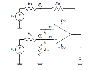
Terminal voltages and currents are used to characterize $\mathrm{OpAmp}$ behavior. In order to unify all discussions of $\mathrm{OpAmp}$ circuitry, it is necessary to define appropriate descriptive conventions. All voltages are measured relative to a common reference node (or ground) which is external to the chip as is shown in Figure 1.4. The voltage between the inverting pin and ground is denoted as $v_1$ : the voltage between the non-inverting pin and ground is $v_2$. The output voltage referenced to ground is denoted as $v_o$. Power is typically applied to an $\mathrm{OpAmp}$ in the form of two equalmagnitude supplies, denoted $V_{C C}$ and $-V_{C C}$, which are connected to the $\mathrm{V}^{+}$and $\mathrm{V}^{-}$terminals of the OpAmp, respectively.
The reference current directions are shown in Figure 1.4. The direction of current flow is always into the nodes of the $\mathrm{Op}{\mathrm{p}}$ Amp. The current into the inverting input terminal is $i_1$; current into the non-inverting input terminal is $i_2$; current into the output terminal is $i_o$; and the currents into the positive and negative power supply terminals are $I{C-}$ and $I_{C+}$, respectively.
The voltage and current constraints inherent to the input and output terminals of an OpAmp must be understood prior to connecting external circuit elements. The OpAmp is considered as a building block element with specific rules of operation. A short discussion of these rules of operation follows. The terminal voltages are constrained by the following relationships ${ }^5$ $$ v_o=A\left(v_2-v_1\right) $$ and $$ -V_{C C} \leq v_o \leq V_{C C} \text {. } $$ The first of the two voltage constraints states that the output voltage is proportional to the difference between the non-inverting and inverting terminal inputs, $v_2$ and $v_1$, respectively.
电气工程代写|数字电路代写digital circuit代考|OPERATIONAL AMPLIFIERS AND APPLICATIONS
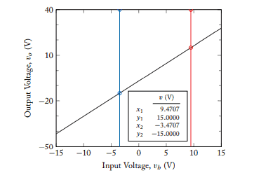
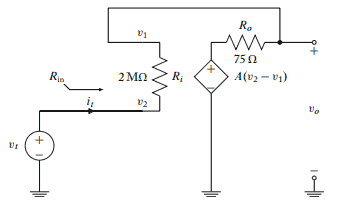
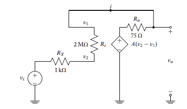
Substituting Equations (1.17) and (1.18) into (1.16) yields $$ i_t=\frac{v_t-A i_t R_i}{R_i+R_o} . $$ The Thévenin input resistance, $R_{\text {in }}$, is found by rearranging Equation (1.19), $$ R_{i n}=\frac{v_t}{i_t}=R_i(1+A)+R_o . $$ For the given typical parameter values $\left(R_i=2 \mathrm{M} \Omega, A=200 \mathrm{~K}\right.$, and $\left.R_o=75 \Omega\right)$, the input resistance can be calculated to be the very large value: $R_{i n}=400 \times 10^9 \Omega$. It is reasonable to assume that the input resistance of a unity gain buffer, $R_{i n}$ is, for all practical purposes, infinite. Example 1.1 Determine the output resistance of an OpAmp voltage follower. Solution: To find the output resistance, $R_{\text {out }}$, a test voltage source is connected to the output of the voltage follower to find the Thévenin equivalent resistance at the output. Note also that all independent sources must be zeroed. That is, all independent voltage sources are short circuited and all independent currents are open circuited. The circuit used to find $R_{\text {out }}$ is shown in Figure $1.10 .{ }^{10}$ To find the Thévenin equivalent output resistance, a test voltage source, $v_t$ is connected at the output. The circuit draws $i_t$ source current. The input at $v_2$ has been short circuited to ground to set independent sources to zero.
电气工程代写|数字电路代写digital circuit代考|Operational Amplifiers and Applications
The Operational Amplifier (commonly referred to as the OpAmp) is one of the primary active devices used to design low and intermediate frequency analog electronic circuitry: its importance is surpassed only by the transistor. OpAmps have gained wide acceptance as electronic building blocks that are useful, predictable, and economical. Understanding OpAmp operation is fundamental to the study of electronics.
The name, operational amplifier, is derived from the ease with which this fundamental building block can be configured, with the addition of minimal external circuitry, to perform a wide variety of linear and non-linear circuit functions. Originally implemented with vacuum tubes and now as small, transistorized integrated circuits, OpAmps can be found in applications such as: signal processors (filters, limiters, synthesizers, etc.), communication circuits (oscillators, modulators, demodulators, phase-locked loops, etc.), Analog/Digital converters (both A to D and $\mathrm{D}$ to $\mathrm{A}$ ), and circuitry performing a variety of mathematical operations (multipliers, dividers, adders, etc.).
The study of OpAmps as circuit building blocks is an excellent starting point in the study of electronics. The art of electronics circuit and system design and analysis is founded on circuit realizations created by interfacing building block elements that have specific terminal characteristics. OpAmps, with near-ideal behavior and electrically good interconnection properties, are relatively simple to describe as circuit building blocks.
Circuit building blocks, such as the $\mathrm{O}_{\mathrm{p} A} \mathrm{mp}$, are primarily described by their terminal characteristics. Often this level of modeling complexity is sufficient and appropriately uncomplicated for electronic circuit design and analysis. However, it is often necessary to increase the complexity of the model to simplify the analysis and design procedures. These models are constructed from basic circuit elements so that they match the terminal characteristics of the device. Resistors, capacitors, and voltage and current sources are the most common elements used to create such a model: an OpAmp can be described at a basic level with two resistors and a voltage-controlled voltage source.
OpAmp circuit analysis also offers a good review of fundamental circuit analysis techniques. From this solid foundation, the huilding block concept is explored and expanded throughout this text. With the building block concept, all active devices are treated as functional blocks with specified input and output characteristics derived from the device terminal behavior. Circuit design is the process of interconnecting active building blocks with passive components to produce a wide variety of desired electronic functions.
One of the fundamental characteristics of an amplifier is its gain. ${ }^1$ Gain is defined as the factor that relates the output to the input signal intensities. As shown in Figure 1.1, a time dependent input signal, $x(t)$, is introduced to the “black box” which represents an amplifier and another time dependent signal, $y(t)$, appears at the output. Figure 1.1: “Black box” representation of an amplifier with input $\mathbf{x}(t)$ and output $\mathbf{y}(t)$. In actuality, $\mathbf{x}(t)$ can represent either a time dependent or time independent signal. The output of a good amplifier, $\mathbf{y}(t)$, is of the same functional form as the input with two significant differences: the magnitude of the output is scaled by a constant factor, $A$, and the output is delayed by a time, $t_d$. This input-output relationship can be expressed as: $$ \mathbf{y}(t)=A \mathbf{x}\left(t-t_d\right)+\alpha $$ Where $A$ is the gain of the amplifier, $\alpha$ is the output DC offset, and $t_d$ is the time delay between the input and output signals. The signal is “amplificd” by a factor of $A$. Amplification is a ratio of output signal level to the input signal level. The output signal is amplified when $|A|$ is greater than 1 . For $|A|$ less than 1 , the output signal is said to be attenuated. If $A$ is a negative value, the amplifier is said to invert the input. Should $x(t)$ be sinusoidal, inversion of a signal is equivalent to a phase shift of $180^{\circ}$ : negative $A$ implies the output signal is $\pm 180^{\circ}$ out of phase with the input signal.
For time-varying signals, it may be convenient to find the amplification (ratio) by comparing either the root-mean-squared (RMS) values or the peak values of the input and output signals. Good measurement technique dictates that amplification is found by measuring the input and output RMS values since peak values may, in many instances, be ambiguous and difficult to quantify. ${ }^2$ Unfortunately, in many practical instances, RMS or power meters are not available dictating the measurement of peak amplitudes. The delay time is an important quantity that is often overlooked in electronic circuit analysis and design. ${ }^3$ The signal encounters delay between the input and output of an amplifier simply because it must propagate through a number of the internal components of the amplifying block.